
Circuits At the Nanoscale: Communications, Imaging & Sensing (Edited by Krzysztof Iniewski)

Overview
This technical text explores the evolution of complementary metal oxide semiconductor (CMOS) technology as it advances into the nanoscale era, focusing on the transition from simple device shrinking to complex system-on-chip (SoC) integration. The source details how the semiconductor industry is moving beyond the traditional "shrink path" defined by Moore’s Law to address physical limitations like gate leakage and variability through innovations such as high-k metal gates and strained silicon. It categorizes the current landscape into "plain vanilla" CMOS for logic and "CMOS+" for specialized applications in communications, imaging, and sensing, including RF and high-voltage technologies. Ultimately, the text serves as a comprehensive guide for engineers to navigate manufacturability challenges and design-for-yield strategies, ensuring that silicon remains a versatile platform for diverse modern electronics.
Expand for Additional Links
Unable to Find Page: /quantum/semiconductors.html in Collection quantum The Collection is Valid useFinder is falseUnable to Find Page: /technical/crystals.html in Collection technical The Collection is Valid useFinder is falseUnable to Find Page: /reading/crystals-atlantis.html in Collection reading The Collection is Valid useFinder is falseUnable to Find Page: /reading/nano-berg.html in Collection reading The Collection is Valid useFinder is false

The Nanoscale Revolution: A Guide to Semiconductor Evolution and Scaling Laws
1. The Historical Torch-Pass: From Bipolar to CMOS Dominance
We must view the history of the semiconductor industry not as a mere timeline of inventions, but as a series of manufacturing triumphs. The Field-Effect Transistor (FET) was actually the first concept proposed in the 1930s, yet it remained a theoretical ghost because the materials science of the era could not physically realize it. Consequently, the Bipolar Junction Transistor (BJT) took the lead, earning its inventors the Nobel Prize and dominating the 1960s. However, as we moved through the PMOS and NMOS revolutions of the 1970s, the industry eventually crowned the Complementary Metal Oxide Semiconductor (CMOS) as the king of logic in the 1990s.
The Transistor Evolution
| Era | Dominant Technology | Defining Characteristic |
|---|---|---|
| 1930s–1950s | Theoretical FET | Proposed early but physically unbuildable with current materials. |
| 1960s | Bipolar (BJT) | Current-controlled; high speed but high power consumption. |
| 1970s–1980s | PMOS / NMOS | Introduction of MOS; focus on N-channel performance and density. |
| 1990s–Present | CMOS | Voltage-controlled; ultra-low standby power; the industry standard. |
The "Magic" of Voltage Control The pivot to CMOS was driven by a fundamental shift in device physics: how we control the flow of electricity.
- Current-Controlled (Bipolar): Think of this as a water tap that requires the water to be flowing with significant pressure just to detect that the valve is open. You cannot have a high base-emitter voltage (Vbe) without significant current flow.
- Voltage-Controlled (CMOS): This is the secret to modern efficiency. CMOS acts like a static pressure gauge; you can maintain a high gate-source voltage (Vgs) to control the device while essentially drawing zero current. This characteristic is what allows your smartphone to sit in your pocket for hours without draining its battery.
This inherent efficiency provided the foundation for specific scaling principles that fueled the exponential growth of the digital age.
2. The Three Pillars of the CMOS Era
As identified by Paul Rousseau, the rise of CMOS to its status as the "800 lb gorilla" of technology was supported by three fundamental pillars.
I. Low Standby Power First proposed by Frank Wanlass at Fairchild in 1963, this pillar addresses the "waste" of a device when it isn't working. CMOS only draws significant power during the act of switching, making it the ideal building block for complex processors.
Learner's Note: Imagine a light switch that only consumes electricity at the exact micro-second your finger flips it, rather than burning energy just by being in the "on" position.
II. Dennard Scaling Articulated by Robert Dennard of IBM in 1974, this principle was the "magic wand" of engineering. It proved that as MOS transistors are scaled down, they simultaneously become faster and use less power.
Learner's Note: Scaling was the only "free lunch" in physics—making a device smaller actually improved every single performance metric at once.
III. Manufacturability CMOS succeeded because the industry created a "well-oiled ecosystem" of foundries, design tools, and intellectual property. It wasn't just a better transistor; it was a transistor that could be built by the billions with high reliability.
Learner's Note: Innovation requires more than a brilliant idea; it requires a repeatable, affordable factory system—the ecosystem—capable of global-scale production.
While these pillars supported decades of progress, we have recently hit physical and economic "brick walls" that require a complete reengineering of the transistor.
3. The Scaling Crisis: Leakage and Modern Remedies
As we pushed transistors toward the nanoscale, the "free lunch" of Dennard scaling ended. We encountered "clouds on the horizon" where power supply voltages stopped scaling downward and heat became unmanageable. The crisis was driven by leakage—electricity bleeding through the device even when it is turned "off." In a sobering benchmark for students, modern CMOS gate leakage has actually approached the levels of a Bipolar base current, signaling the end of the traditional "static" advantage.
Primary Types of Leakage
- Isolation Leakage: Electricity escaping between separate devices on the silicon substrate.
- Gate Leakage: Current tunneling through the gate oxide as it becomes thin enough to be measured in atomic layers.
- Gate-Induced Drain Leakage (GIDL): Leakage caused by high electric fields at the gate-to-drain overlap.
Engineering Solutions to Keep Moore's Law Alive
To survive, the industry moved from simple "shrinking" to fundamental materials reengineering:
- Strained Silicon: By physically stretching or compressing the silicon lattice, we boost the mobility of charge carriers, increasing speed without needing to shrink the footprint.
- High-k Metal Gate (HKMG): This was a dramatic "heart transplant" for the transistor. By replacing silicon dioxide with hafnium-based "high-k" dielectrics and metal gates, we created a barrier that is physically thicker (blocking leakage) but electrically "thinner" (maintaining control).
This shift moved the battlefield from pure materials science to the immense challenges of microscopic imaging.
4. The Manufacturing Barrier: Closing the Subwavelength Gap
We have entered an era called the Subwavelength Gap. This is a manufacturing paradox: we are trying to print transistor features that are significantly smaller than the wavelength of the light we are using to image them. Imagine trying to draw a microscopic, perfectly straight line using a thick, blunt crayon.
The Rayleigh Scaling Equation
The fundamental limit of our "printing press" is governed by the Rayleigh equation: R =
- R (Resolution): The minimum possible linewidth we can print.
: The "process aggressiveness" factor (lower is better, but harder). (Lambda): The wavelength of the imaging light (currently 193nm). - NA (Numerical Aperture): The light-gathering power of the lens.
Next-Generation Lithography Solutions
| Technique | Primary Challenge/Limit |
|---|---|
| Immersion Lithography | Limited by the refractive index (n) of the fluid used between the lens and wafer. |
| Double-Patterning (DPT) | Doubles the cost and time; requires complex layout changes to split patterns. |
| Extreme Ultraviolet (EUV) | Requires specialized mirrors as light is absorbed by almost all materials. |
| Nano-Imprint Lithography (NIL) | Struggles with "overlay"—the precise alignment of one layer on top of another. |
As our printing press becomes less deterministic, the era of the "perfect" transistor ends, and the era of statistical design begins.
5. Variability and the "Correct by Construction" (CBC) Response
Variability is the ghost in the machine—the difference between the blueprint and the final silicon. We categorize these as Within-Die (WID) and Die-to-Die (D2D) variations.
Comparison of Variability Sources
| Random Sources (Stochastic) | Systematic Sources (Deterministic) |
|---|---|
| Line-Edge Roughness (LER): Jaggedness on the gate edges at the atomic level. | Proximity Effects: How the "neighborhood" of nearby shapes distorts a specific line. |
| Doping Fluctuations: The random placement of individual dopant atoms. | Lens Aberrations: Imperfections in the optics (like astigmatism or coma). |
The "Correct by Construction" (CBC) Rules of Thumb
To ensure high yield, we now design layouts that are inherently "easy" for the factory to build.
- The 4
Rule: We add "dummy" lines around sensitive devices up to a "screening distance" of four times the wavelength to ensure the optical neighborhood remains consistent. - The 4x Sizing Rule: For critical analog components, we make geometries four times larger than the minimum allowed size to ensure stability and matching.
Eventually, once we can no longer shrink transistors in a 2D plane, we must change our perspective and look upward.
6. The Final Frontier: Wafer-Level 3D Integration
3D integration is the move from flat "neighborhoods" of transistors to dense "skyscrapers" of functionality. By stacking layers vertically, we solve the "interconnect delay"—the time a signal wastes traveling across a massive, flat chip.
Three 3D Platform Comparisons
- FEOL (Front-End-of-the-Line): Built early in the fabrication process.
- Pro: Highest interconnect density; smallest vias.
- Con: Severe thermal budget issues; the industry lacks a method to create high-quality single-crystal silicon in upper strata.
- BEOL (Back-End-of-the-Line): Wafers are bonded after the transistors are completed.
- Pro: Allows "heterogeneous integration" (e.g., stacking a memory wafer on a logic wafer).
- Con: Requires extreme precision in wafer thinning and alignment.
- WLP (Wafer-Level Packaging): Uses traditional packaging techniques like flip-chip.
- Pro: Easiest to implement with existing factory tools.
- Con: Lowest via density; not truly scalable for advanced logic.
Technical Highlights
- Through-Silicon Vias (TSVs): These are microscopic vertical "elevators" that provide electrical pathways through the silicon bulk to connect the strata.
- BCB Adhesive Bonding: Utilizing Benzocyclobutene as a high-strength dielectric "glue" to secure wafers together before vertical interconnection.
7. Conclusion: The Future of the CMOS Platform
CMOS remains the "800 lb gorilla" because of its massive ecosystem. While "Plain Vanilla CMOS" continues to drive standard digital logic, the frontier of innovation is CMOS+, where specialized functions are grafted onto the standard process rootstock.
To visualize the future, consider the Interstate Highway metaphor: Plain Vanilla CMOS is the Interstate Highway system—vast, fast, and highly standardized. CMOS+ represents the local roads and specialized exits that allow the highway to reach specific, high-value destinations.
The Varieties of CMOS+:
- Embedded Memory: Integrating DRAM or Flash directly into the logic flow for massive bandwidth.
- Image Sensors (CIS): Turning CMOS into the "eyes" of modern devices.
- RF & SiGe BiCMOS: Specialized "flavors" like SiGe BiCMOS enable high-dynamic-range power amplifiers for wireless communication.
Takeaway Insights for the Student
- CMOS is a Platform: It is the universal connector. Even if you invent a non-CMOS "spin device," you will likely need to connect it to a CMOS chip to make it useful.
- Power is the New Timing: Design is no longer just about how fast a signal travels; it is about "power closure"—managing the heat and leakage that threaten to melt the chip.
- The 3D Mindset: The next generation of engineers will not design flat circuits; they will architect complex vertical systems-in-package, moving from 2D sprawl to 3D skyscrapers.
Deep-Submicron Design Standards Handbook: Nanometer CMOS Manufacturability and Variability Control
1. The Nanoscale CMOS Paradigm: Dominance and Scaling Limitations
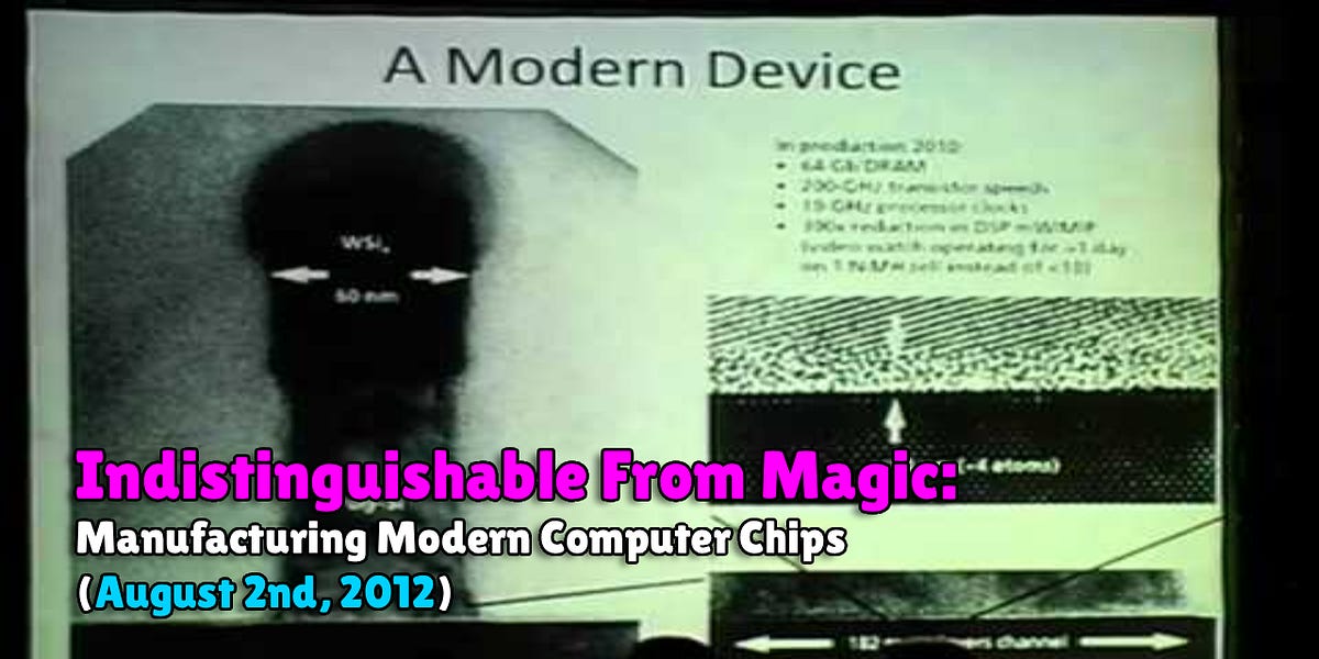
The ascendancy of Complementary Metal Oxide Semiconductor (CMOS) technology to industry dominance was driven by its inherent efficiency as a logic driver, primarily due to its exceptionally low standby power and the scaling methodology established by Dennard’s rules. However, as the industry transitions into the nanometer regime, the traditional scaling of silicon dioxide (SiO₂) gate oxides has reached a fundamental physical limit of 10–15 Å. At these dimensions, gate leakage becomes prohibitively high, directly approaching the levels of a bipolar base current. This crisis has necessitated a strategic shift in semiconductor engineering, moving away from simple dimensional shrinking toward fundamental material and structural innovations to maintain the performance gains expected of modern integrated circuits.
Comparative Rationale: Voltage vs. Current Control
The strategic advantage of CMOS lies in its operation as a voltage-controlled device. Unlike bipolar transistors, which are current-controlled and require a continuous base current to remain active, CMOS allows for a high gate-source voltage (
| Feature | CMOS Voltage Control | Bipolar Current Control |
|---|---|---|
| Control Mechanism | Voltage ( | Current ( |
| Standby Power | Low (ideally zero) | High (continuous base current) |
| Gate/Base Leakage | Approaches bipolar base current at 10–15 Å | Inherent to device operation |
| Scaling Efficiency | High (historically) | Limited by power density |
The Scaling "Cloud" and the Power Problem
Historical scaling laws have encountered a significant obstacle: the abandonment of power supply voltage
Section Transition: While these circuit-level strategies manage the power envelope, the fundamental leakage problem at the 45nm node required a reengineering of the transistor gate stack itself through High-k Metal Gates (HKMG) and strained silicon.
2. Materials Engineering: High-k Metal Gates (HKMG) and Strained Silicon
At the 45nm node, the industry reached a tipping point where traditional SiO₂ dielectrics could no longer prevent excessive gate leakage. Material-level reengineering became a strategic necessity to preserve the viability of CMOS scaling. The introduction of High-k Metal Gate (HKMG) technology represents a complete reengineering of the transistor core to restore control over leakage.
HKMG Implementation Rationale
The adoption of hafnium-based high-k dielectrics increases the permittivity of the gate stack, allowing for a physically thicker layer that reduces tunneling leakage while maintaining high capacitive coupling. When paired with metal gates, this configuration eliminates threshold voltage pinning and phonon scattering. The resulting performance outcomes are significant: drive currents at 1.2V reach approximately 1.75 mA/µm for NMOS and 1.06 mA/µm for PMOS, enabling high-speed operation with minimal off-state current
Performance Optimization through Strain and Silicide
To further boost drive current
- So What? Layer: The primary trade-off in FUSI implementation is the risk of Nickel (Ni) penetration through thin oxides, which causes catastrophic device failure. Furthermore, architects must be aware of a critical characterization risk: incomplete silicidation results in electrical signatures that are frequently misinterpreted by characterization tools as a shift in the gate work function, leading to unpredicted and difficult-to-trace variations in threshold voltage
.
Section Transition: While HKMG and strained silicon address intrinsic material limitations, the geometric challenges of patterning these nanometer features introduce the "subwavelength gap," necessitating aggressive lithographic protocols.
3. Lithography and the Subwavelength Gap
In modern fabrication, the industry faces the "subwavelength gap," where the imaging wavelength (typically 193nm) is significantly larger than the critical dimensions (CD) of the features being printed. This gap necessitates aggressive and complex patterning techniques to maintain yield and pattern fidelity.
Patterning Technology Analysis
| Technology | Resolution | Key Issues | Target Timeframe |
|---|---|---|---|
| Immersion | 0.25 | Max n value limits | Current (65nm/45nm) |
| Dual-Patterning (DPT) | 0.125 | Doubles cost (masks/time) | 32nm and below |
| Nano-imprint (NIL) | N/A | Poor overlay accuracy | 22nm or less |
| Extreme UV (EUV) | 0.8 | Mirrors, light sources | Future nodes |
Resolution Optimization
Resolution (R) is governed by the Rayleigh scaling equation:
- Manipulation of
: This is achieved through Optical Proximity Correction (OPC) and Phase-Shift Masks (PSM). - Numerical Aperture (NA): It is critical to note that while
is a process-controlled variable, the NA is a fixed function of the scanner hardware (e.g., immersion optics). This hardware constraint sets the physical context for how aggressively must be manipulated.
So What? Layer: The evolution of Design-for-Manufacturability (DfM) has transitioned from manual layout sizing to model-based OPC. This shift is critical for preventing "line-end pullback." In the context of nanometer MOSFETs, this pullback directly threatens the integrity of gate end caps, potentially failing to cover active areas and leading to misalignment leakage.
Section Transition: Even with highly optimized lithography, spatial variations across the wafer and within the die introduce deterministic and random fluctuations that require a formal variability framework.
4. Managing Device Variability: WID and D2D Frameworks
Process fluctuations are now a primary roadblock to scaling. As dimensions shrink, the lack of proportional control over process tolerances leads to a proliferation of design corners, requiring designers to manage increasingly large margins to ensure functional silicon.
Variability Taxonomy
Variability must be categorized by parameter and source to apply effective mitigation strategies.
| Parameter | Random Source | Systematic Source |
|---|---|---|
| Channel Dopant | Doping fluctuations | Non-uniform implantation/diffusion |
| Gate Oxide | Si/SiO_2 interface roughness | Non-uniform oxide growth |
| Gate Length | Line-Edge Roughness (LER) | RET, OPC, Proximity, Etching |
Spatial Correlation Mapping
Measurement data distinguishes between Die-to-Die (D2D) and Within-Die (WID) variations.
- Radial Patterns: Wafer maps frequently show a radial pattern of frequency and leakage, attributed to non-uniform resist development during the post-exposure bake (PEB).
- WID Correlation: Gates placed parallel to each other show higher correlation due to the slit-of-light scanning mechanism in the lithography tool. Features aligned with the horizontal slit are subject to lens aberrations, while those aligned with the scan direction are subject to vibration and dosage variations.
Layout-Driven Impact
The density and pitch of poly-Si gates profoundly impact performance. Isolated gates tend to print shorter than dense gates, leading to a systematic frequency shift of up to 10% and a leakage increase of up to 20x. Crucially, dense lines exhibit a higher depth of focus, making them more immune to the defocusing of optical systems and providing greater stability compared to isolated structures.
Section Transition: Mitigating these variations requires moving from reactive CAD fixes to proactive "Correct-by-Construction" (CBC) primitives.
5. Correct-by-Construction (CBC) and Yield Enhancement Protocols
CBC primitives limit the design space to highly manufacturable, standardized layouts, reducing the WID variability margin from 10% to under 2%.
Layout Standardization and the 4x Rule
Low-variability layout focuses on on-grid, one-dimensional (1D) straight lines. A critical rule of thumb for sensitive designs is the 4x Rule: ensuring that critical geometries are four times larger than the minimum process capability. This raises the
Pattern Density and Waffling
Non-uniform pattern density leads to "dishing" during Chemical-Mechanical Polishing (CMP) and variations in Interlayer Dielectric (ILD) thickness.
- Geometric Waffling: Standard automated filling that adds fixed-density structures; often inefficient and raises parasitic capacitance.
- Intelligent Waffling: A refined approach that matches dummy structures to pre-existing die-level pattern density. This method is vital for vertical CD control, as it reduces the ILD thickness difference (D) from over 400nm to under 200nm.
Dummy Structure Protocols
To mitigate 2D variability, a Dummy Feature Ring (DRW) is required. The screening distance for these features is defined as
Section Transition: While 2D layout optimization is vital for yield, 3D integration offers a new dimension for functional density and parasitic reduction.
6. Advanced Integration: Wafer-Level 3D Platforms
As 2D scaling hits diminishing returns, the industry is transitioning toward 3D integration enabled by Through-Silicon Vias (TSVs). This reduces interconnect parasitics—specifically inductance—compared to traditional wire bonding.
Platform Evaluation
- FEOL Platforms: Device layers formed early (e.g., epitaxial overgrowth). Offers the highest density with 100nm vias, but faces severe thermal budget challenges.
- BEOL Platforms: Bonding of separately fabricated wafers. Currently the most viable path for heterogeneous integration.
- WLP Platforms: Packaging-based stacking (e.g., flip-chip). Limited by significantly larger via sizes (20–40µm), restricting interconnect density.
Bonding Technology Comparison
| Feature | Copper-to-Copper (Cu-to-Cu) | Dielectric Adhesive (BCB) |
|---|---|---|
| Bond Strength | Moderate (requires grain growth) | High |
| Alignment | Critical for via-first contact | Flexible (via-last compatible) |
| Seal Rings | Mandatory (to prevent oxidation) | Generally unnecessary |
| Process Flow | Typically "Via-First" | Typically "Via-Last" |
So What? Layer
The choice between process flows is a strategic cost-benefit decision. Via-First flows allow for the highest interconnect density but require extreme wafer planarity, representing a primary manufacturing yield risk. Via-Last flows using BCB are more robust and cost-effective, as they accommodate higher surface topography while still providing significantly lower parasitics than packaging-level 3D solutions.
Final Summary
Reliable, high-yield nanometer manufacturing requires a holistic synthesis of material innovation (HKMG), rigorous DfM/CBC protocols to manage spatial variability, and advanced 3D integration. By transitioning from simple shrinking to a methodology focused on variability control and vertical scaling, architects can continue to deliver the performance required for the next generation of silicon systems.
Strategic Assessment of CMOS and CMOS+ Integration Platforms for Large-Scale Manufacturing
1. The Evolution and Economic Dominance of the CMOS Ecosystem
The ascent of Complementary Metal Oxide Semiconductor (CMOS) technology to market hegemony is more than a technical milestone; it is the construction of an insurmountable moat. CMOS acts as the gravitational center for all silicon investment, effectively de-risking secondary "flavored" integrations by leveraging a well-oiled ecosystem that commands $200+ billion in annual logic wafer sales. This massive economic footprint ensures that every dollar of R&D, capital expenditure (CapEx), and Electronic Design Automation (EDA) development is prioritized for CMOS, creating a formidable barrier for any contender technology. Historically, the transition from current-controlled bipolar devices to voltage-controlled CMOS was mandated by the strategic necessity of low standby power and the predictable density gains of Dennard scaling.
The Pillars of Dominance
The strategic entrenchment of CMOS rests on three critical technical and economic pillars:
- Strategic Power Efficiency: As a voltage-controlled current device, CMOS allows high gate-source voltage (
) without significant current flow—a property that current-controlled bipolar devices cannot replicate without massive power penalties. - The Scaling Imperative: Adherence to Dennard’s rules facilitated decades of density improvements. Even as scaling laws are modified to include high-k metal gates (HKMG) to manage atomic-scale leakage, the ecosystem's momentum remains unbroken.
- Systemic Manufacturability: The development of affordable, high-volume processes has turned CMOS into the primary technology driver for the global semiconductor industry, de-risking the path for high-complexity designs.
At the 65nm technology node, the economic efficiency of CMOS reaches a staggering scale: $1 can purchase more than 10 million transistors. This valuation includes up to eight levels of copper interconnects, effectively rendering the cost of individual wires a negligible fraction of a microcent and making "interconnect-heavy" architectures economically viable.
This logic-centric foundation serves as the "root stock" for the industry. However, the modern market's demand for diversified functionality necessitates a shift from "plain vanilla" CMOS to specialized variants, complicating the roadmap for system architects.
2. Comparative Evaluation of Specialized CMOS+ Platforms
As consumer applications diversify, "plain vanilla" CMOS logic is no longer a catch-all solution. To address this, the industry grafts specialized "flavors" onto the standard CMOS root stock, a paradigm known as CMOS+. This strategy allows manufacturers to exploit existing CMOS infrastructure while integrating niche capabilities such as memory, high voltage, or imaging.
Platform Differentiation
| Platform | Key Features & Strategic Advantages | Comparison vs. Standard Logic/Alternatives |
|---|---|---|
| Logic-Based eDRAM | High memory bandwidth; 2–3x denser than SRAM; reduced active/standby power. | Avoids power penalties of off-chip I/O; logic suffers no performance penalty beyond cost. |
| Embedded Flash | Enables microcontrollers; utilizes logic-identical OTP/MTP solutions for chip ID/trimming. | Limited by 80–100 Å gate oxide thickness; scaling is significantly more difficult than pure logic. |
| High-Voltage CMOS (HV) | Integrates DDD/LDMOS or BCD (Bipolar CMOS DMOS) for power and LED/LCD drivers. | Breathes new life into mature 0.18µm lines; leverages silicon-proven IP to reduce R&D risk. |
| Image Sensors (CIS) | Lower voltage and higher speed than CCDs; integrates pixel processing on-chip. | Does not require a dedicated fab; leverages existing logic manufacturing for rapid ramp-ups. |
| RF CMOS and SiGe BiCMOS | CMOS handles WLAN/Bluetooth at low cost; SiGe offers higher dynamic range/power. | CMOS provides |
While these diversifications expand the utility of the platform, they necessitate rigorous variability management, as "flavored" processes introduce non-deterministic manufacturing complexities.
3. Manufacturability and Variability in Deeply Scaled Nodes
In the sub-100nm regime, we have shifted from a traditional "shrink path" to a periphery-centric development model. Manufacturing is no longer a deterministic exercise; it is an interaction of lithography, etch profiles, and material physics. This shift makes Design-for-Manufacturability (DfM) the primary gatekeeper for yield.
Closing the Subwavelength Gap
As feature sizes shrink below the 193nm wavelength of imaging light, a "subwavelength gap" emerges. Lithography must manage the
Where R is the minimum-resolved linewidth, \lambda is wavelength, and NA is numerical aperture. While aggressive Optical Proximity Correction (OPC) can drive
Variability Taxonomy
Strategic architects must distinguish between systematic and random variations to optimize design margins:
| Variation Category | Primary Source | Strategic Impact |
|---|---|---|
| Within-Die (WID) | Lens aberrations (astigmatism, coma), flare, and local pattern density. | Affects spatial correlation; parallel gates show higher correlation than scanned features. |
| Die-to-Die (D2D) | Thermal profiles during postexposure bake (PEB) and resist development. | Often results in radial patterns; center dies are frequently faster and leakier. |
| Random Variations | LER (Line-Edge Roughness) and Dopant Fluctuations ( | Fundamental roadblocks to scaling; cannot be modeled deterministically. |
Mitigation and the CBC Methodology
To ensure high parametric yield, the Correct by Construction (CBC) methodology is the operational solution. By using standardized, pre-approved layout primitives, we circumvent the lithography gap.
- The 4x Rule of Thumb: For high-precision analog/RF use, any geometry should be 4x larger than the minimum process capability CD to ensure a
factor in the 0.6–1.0 range. - Dummy Structures: Using dummy feature rings (DRW =
) mitigates 2D variability, though it requires careful extraction to manage parasitic capacitive coupling.
4. Strategic Decision-Making: SoC vs. SiP vs. 3D Integration
The choice between System-on-a-Chip (SoC) and System-in-Package (SiP) is a high-stakes balance of cost, risk, and Schedule Readiness.
- The Schedule Readiness Trap: "Plain vanilla" logic is always available first on a new node. Choosing CMOS+ (SoC) integration often forces a product into a lagging node because specialized masks and processes (like HV or Flash oxide steps) are not ready at the same time as the baseline 22nm or 45nm logic.
- Performance vs. Flexibility: While SoC provides higher bandwidth and lower active power, SiP allows for the integration of incompatible technologies (e.g., MEMS) without the CapEx risk of a custom CMOS+ process.
Wafer-Level 3D Integration Platforms
For systems requiring extreme density, 3D platforms offer a path beyond 2D scaling limits:
- Front-End (FEOL): Highest density (100nm vias) but suffers from thermal budget challenges that degrade device quality in upper strata.
- Back-End (BEOL): Utilizing Through-Silicon Vias (TSVs) and BCB dielectric adhesive bonding. Crucially, TSVs provide significantly decreased interconnect parasitics, particularly inductance, which is a decisive advantage for high-speed logic and analog interfaces.
- Wafer-Level Packaging (WLP): Uses micro flip-chip solder bumps (20–40µm). While cost-effective today, it lacks the scalability required for the 22nm node and beyond.
Economic Implications for CapEx
CapEx planning must prioritize the logic-first reality. The decision to invest in CMOS+ complexity must be weighed against the schedule risk. For many innovators, the most efficient path is leveraging existing foundry infrastructure rather than funding boutique fabs.
5. Conclusions and Forward-Looking Guidance
The CMOS ecosystem functions as the "interstate highway system" of the semiconductor world—a fast, efficient, and heavily invested infrastructure. CMOS+ variants act as the local highway networks, extending this reach into specialized territories. To lead in this environment, architects must follow a disciplined integration roadmap.
Strategic Directives
- Leverage Depreciated Assets: CMOS+ breathes new life into mature manufacturing lines. Strategists should prioritize implementing specialized functions on depreciated 0.18µm or 90nm lines where the CapEx is already sunk and the IP is silicon-proven.
- Adopt Correct by Construction (CBC): Avoid "boutique" layout styles. Use standardized primitives and the 4x rule for critical paths to minimize WID variability and ensure first-pass success.
- Prioritize Foundry Strategy: Avoid the massive overhead of dedicated fabs. Only move to custom CMOS+ when the performance benefit of reduced parasitic inductance (via TSVs) or density clearly outweighs the schedule lag of being on a non-vanilla logic node.
By leveraging the multi-billion dollar global investment in CMOS, we drive proprietary innovation on the back of the most efficient manufacturing platform ever devised.
The Nanoscale Revolution: How CMOS Powers the Modern World
1. The Invisible Giant: An Introduction to CMOS
In the landscape of modern electronics, the Complementary Metal Oxide Semiconductor (CMOS) is the "interstate highway system" of our digital existence. Just as highways provide the essential infrastructure for global commerce, CMOS provides the foundational platform upon which almost all modern digital logic, sensing, and communication systems are built.
The journey to CMOS dominance was a strategic evolution. While the 1960s were the decade of Bipolar technology, the 1970s saw the introduction of PMOS and NMOS. By the 1990s, CMOS had established itself as the "king of logic" for three primary reasons:
- Low Standby Power: CMOS circuits consume very little power when not actively switching, making them the gold standard for battery-operated devices.
- Scaling Efficiency: CMOS can be shrunk (scaled) more effectively than Bipolar technology, allowing for denser integration without a catastrophic increase in heat.
- Manufacturability: The industry developed a highly reliable, high-yield, and affordable ecosystem for mass-producing CMOS at an unprecedented scale.
"In 65 nm technology, $1 can purchase well over 10 million transistors. This cost includes eight levels of copper wiring to interconnect them, meaning each wire costs a fraction of a microcent."
While CMOS began as a platform for computer logic, it has matured into a versatile rootstock, allowing engineers to graft on specialized "flavors" of technology to meet the demands of a connected world.
2. The Logic of Dominance: Why CMOS Wins
The primary reason CMOS wins is its fundamental physics: it is a voltage-controlled device. By using a voltage at the gate to control the flow of current, rather than using a continuous current to control another current (as Bipolar does), CMOS maintains an efficiency Bipolar cannot touch.
| Feature | CMOS Characteristic | Learner's Benefit |
|---|---|---|
| Power Control | Voltage-controlled current device. | Zero current flow even with high gate-source voltage (Vgs); saves battery. |
| Scalability | Follows predictable scaling laws. | Higher performance and lower cost-per-transistor with every generation. |
| Logic Density | Massive integration (billions of gates). | Complex "Lego sets" for designers to build GPUs and SoCs on one chip. |
As we reached the nanoscale, the industry faced "gate leakage," where the insulating layers became so thin that electricity began to seep through. The solution was the High-k Metal Gate (HKMG)—a complete reengineering of the transistor's heart that restored control and allowed scaling to continue. This adaptability has transformed "plain vanilla" CMOS into a specialized toolkit known as CMOS+.
3. The Specialist’s Toolkit: CMOS+ and Embedded Systems
By modifying the standard CMOS process, we create specialized variants that handle memory and power management on the same chip as the digital "brain."
- Embedded DRAM: There is a critical distinction here between "DRAM-based logic" and logic-based DRAM. Older DRAM processes limited gate oxide scaling to 30–40 Å, which penalized performance. By using a logic-based process, we keep the transistors "fast" and achieve massive memory bandwidth while avoiding the power-hungry I/O transistors required to talk to off-chip memory.
- Embedded Flash: Essential for microcontrollers and security, this variant uses a floating gate mechanism. Because the floating gate requires a thicker oxide (at least 70 Å) to hold a charge, these variants often necessitate 3.3V I/O transistors, providing non-volatile memory for security IDs and smart cards.
- High-Voltage CMOS: This allows digital logic to interact with the physical world. It uses LDMOS structures to drive LCD displays and MEMS, acting as the interface between silent digital logic and high-power applications like LED lighting.
This toolkit allows devices to do more than just think—it allows them to perceive the world around them.
4. Digital Vision: The CMOS Image Sensor (CIS)
The explosion of mobile photography is a direct result of CMOS integration. While the older Charge-Coupled Device (CCD) offered high image quality, the CMOS Image Sensor (CIS) offered two critical advantages for the smartphone era: low power consumption (operating at less than half the voltage of CCDs) and the ability to integrate the "eye" and the "brain" on a single chip.
Note: To transform a logic chip into an effective "eye," engineers must perform a specialized modification: thinning the back-end metal stack. This physical change ensures that light reaches the pixels efficiently without being blocked by the chip’s own internal wiring.
5. Invisible Threads: RF CMOS and Wireless Connectivity
Beyond sight, CMOS provides the "voice" for modern devices. RF CMOS enables daily protocols like Bluetooth, WLAN (Wi-Fi), and high-speed WiMAX 802.16.
While SiGe BiCMOS (Silicon-Germanium) is a powerful competitor for high-performance "niche" areas like power amplifiers, its dominance is limited. The "evangelist's insight" here is that SiGe allows for a higher power supply at the same speeds as CMOS, providing a larger dynamic range. However, for mass-market integration and cost-efficiency, standard RF CMOS is the undisputed leader.
Common Applications of RF CMOS:
- Bluetooth peripherals and 802.13 protocols.
- Wireless smart-home sensors and UWB.
- Streaming audio/video and 60GHz high-frequency radios.
6. The Vertical Leap: Wafer-Level 3D Integration
As we hit the physical "brick wall" of 2D scaling, the industry is moving from a sprawling suburban "parking lot" layout to a dense "urban skyscraper" model. This is 3D Integration.
The secret to this vertical leap is the Through-Silicon Via (TSV). These are vertical connections that punch through the silicon. Their "so what?" factor is massive: by stacking circuits vertically, we create much shorter interconnects, which drastically decreases the "parasitics" (inductance and capacitance) that slow down traditional chips.
| Platform Type | Key Advantage | Via Size (Scale) | Current Limitation |
|---|---|---|---|
| FEOL (Front-End) | Highest density of interconnects. | 100 nm | Thermal budgets make high-quality upper layers difficult. |
| BEOL (Back-End) | Allows heterogeneous integration. | 1 µm | Requires extreme wafer-to-wafer alignment precision. |
| WLP (Packaging) | Uses established flip-chip techniques. | 20–40 µm | Harder to scale; lower interconnect density. |
To bond these "floors" together, engineers use Benzocyclobutene (BCB). BCB is a unique dielectric adhesive; it acts as both a glue to hold the wafers together and an insulator to keep the circuits separate. It is highly versatile, supporting both "via-first" and "via-last" manufacturing flows.
7. Conclusion: The Versatility Narrative
CMOS is no longer just for computer logic. It has become the universal platform for sensing, seeing, hearing, and communicating. If you are an aspiring technologist, remember the ecosystem is built to support this platform first.
The CMOS Rules of Thumb:
- Integration First: If a new tech is invented, always ask: "Can it be done in CMOS or CMOS+?"
- Leverage the Ecosystem: Using CMOS means you are using the most well-oiled manufacturing machine in history.
- Efficiency over Everything: Whether it is 3D stacking or High-k gates, the goal is always to minimize power while maximizing "grokkable" performance.
Check for Understanding
- Why does the "voltage-controlled" nature of CMOS make it superior to Bipolar technology for modern mobile devices?
- What is the specific physical role of Benzocyclobutene (BCB) in creating a 3D integrated circuit?
- How does moving from off-chip memory to logic-based DRAM improve system performance in terms of memory bandwidth and I/O power consumption?